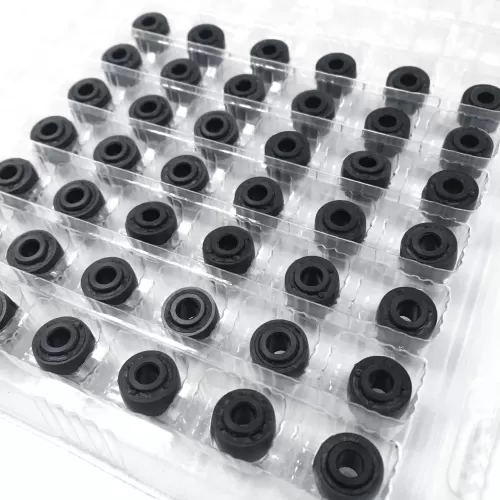
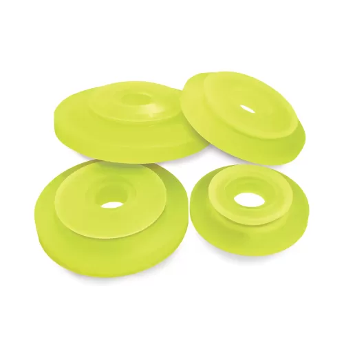
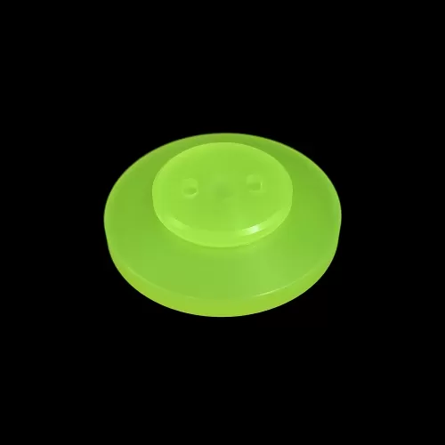
CMP Consumable Parts
CMP stands for Chemical Mechanical Planarization or more commonly Chemical Mechanical Polishing. This is a crucial process technology step for the semiconductor wafer fabrication processes. This step includes the top surface of the wafer to be polished or planarized to build a levelled surface.
CMP Procedure
Chemical mechanical planarization is used widely to remove selected materials for topography planarization including machine formatting and structuring for semiconductor manufacturing. The polishing process is a combination of mechanical and chemical. The mechanical side of the procedure applies pressure downwards whereas, chemical reaction is tailored to match the material that is being processed to eliminate harsh particles.
Perfect Material Quality
We source only from the highest quality suppliers in the world and we train our team on Copy Exact procedures.